20+ ic 555 block diagram
The 555 timer IC is an integrated circuit chip used in a variety of timer delay pulse generation and oscillator applications. An SMPS-switched mode power supply can be used for supplying huge load current by small power.

20 Free Pcb Design Software Pcb Design Software Software Design Pcb Design
The block diagram of a vertical axis wind turbine is shown below.
. The SISO shift register block diagram is shown below which includes 3-D flip-flops. Block Diagram of Pulse Code Modulation. Learning by doing is the best.
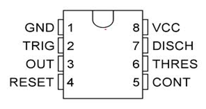
8051 Pin Diagram Description. You may note some pins are designated with two signals shown in. Now lets go through pin configuration in detail.
In this we have eight LEDs that glow one after the other to form a circling effect. Class D power amplifier circuit diagram working waveforms and theory of operation. Here if any obstacle or any object is found that is detected by ultrasonic transducer then it transmits the waves and gets reflected back from the object and.
This block diagram includes a Vertical Axis Wind Turbine VAWT gearbox generator battery LDR circuit and LED. ASCII characters only characters found on a standard US keyboard. Digi-Key is your authorized distributor with over a million in stock products from the worlds top suppliers.
Vertical Axis Wind Turbine Block Diagram. Lets build these circuits. News Stories CPW issues hunting and fishing licenses conducts research to improve wildlife management activities protects high priority wildlife Head to head side by side Robby Gordons innovation is obvious at every level and the base-level packages of each UTV are packed with standard factory features that you just wont find.
Comparator based on an OPAMP switching circuit and a low pass filter. Here is a block diagram of the steps which are included in PCM. The functional block diagram of the IC as a switching regulator is shown below.
Our global writing staff includes experienced ENL ESL academic writers in a variety of disciplines. The proposed system uses 8051 microcontrollers power supplies an ultrasonic transducer module that includes transmitter and receiver LCD display blocks are used which are shown in the above block diagram. Usually its 5V DC.
Keep up with City news services programs events and more. Block diagram 8 pin DIP configuration Pin diagram and description. Class D amplifiers have.
Official City of Calgary local government Twitter account. 555 IC Timer Block Diagram 555 IC Timer Block Diagram. Rated 1 in content and design support.
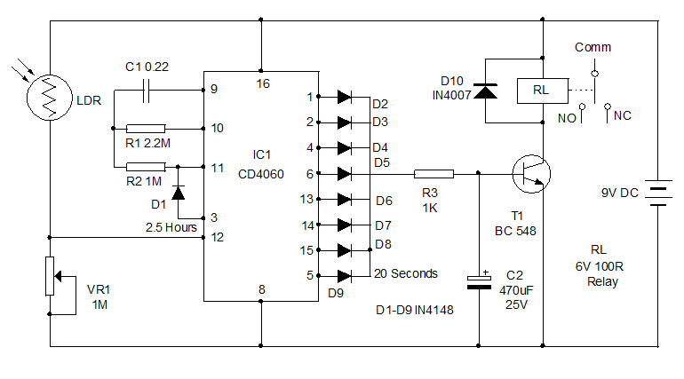
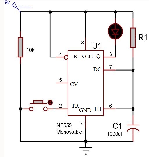
It works in the form of a Monostable or One-shot Operation. A voltage regulator in the regulated power supply is essential for keeping a steady DC output voltage by supplying load regulation as well as line regulation. The design was first marketed in 1972 by.
The power source in the above block diagram offers the necessary energy for the system. Let us look at the pin diagram to have an idea about the timer Integrated Circuit IC before we talk about 555 timer working. The basic block diagram of PCM is given below for better.
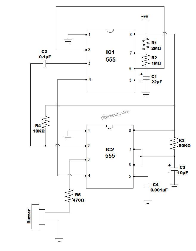
However 555 is still the most popular. My intention in publishing this circuit is not just to make some artwork with electronics but also to illustrate the ic 4017 working principle and circuit design using IC 555 in astable mode 4017 counter and to explain the related concepts. The complete circuit diagram for this Fire Fighting Robot is given below.
Electric Drive Block Diagram Power Source. SISO Shift Register Block Diagram. This circuit is also called a DELAY.
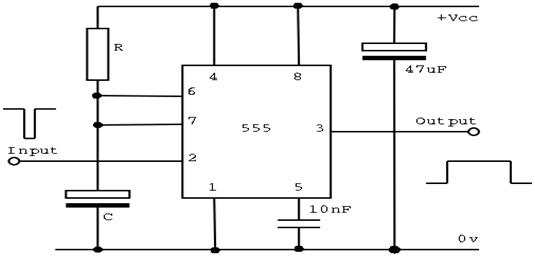
The block diagram of a 555 timer is shown in the above figure. 555 Timer IC 16 8051 26 8051 projects 21 Amplifier Circuits 39. The block diagram of ADC is shown below which includes sample hold quantize and encoder.
A 555 timer has two comparators which are basically 2 op-amps an R-S flip-flop two transistors and a resistive network. The output energy generated from this can be used by any type of load. Must contain at least 4 different symbols.
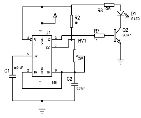
5 circuits of 555 Alarm sound and tone. Both ways the connections are very simple and you should be able to get it right. 555 Sound effect generator circuit.
Named as Vcc is the main power source. The ic 4017 led circuit diagram is shown. This lets us find the most appropriate writer for any type of assignment.
In sampling we are using a PAM sampler that is Pulse Amplitude Modulation Sampler which converts continuous amplitude signal into Discrete-time- continuous signal PAM pulses. Derivatives provide two or four timing circuits in one package. For this reason we can employ regulators like a Zener transistorized otherwise 3-terminal integrated regulators.
Variants consist of combining multiple chips on one board. From the functional diagram we can see that the IC has a comparator circuit with an inverting and on-inverting input along with a 1 volt internal reference to each input which clearly simplifies the circuit design and PCB layout. People know it as the 555 timer IC.
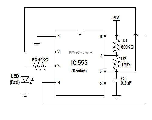
You can either connect all the shown connections for uploading the program to check the working or you can assemble the bot completely and then proceed with the connections. Polaris rzr decal wraps. We can use the 555 as a timer for up to 10 minutes.
Here the automatic lighting system is used as a load. This modulator can be used to control the op power of the supply. The ADC 0808 IC requires a clock signal of typically 550 kHz ADC0808 is used to convert the data into digital form required for the microcontroller.
The block diagram of a Class D amplifier is shown in the figure below. The connection of these FFs can be done by connecting the one Flip Flops output to the next flip flop input. The main features of ADC0804 include the following.
For describing pin diagram and pin configuration of 8051 we are taking into consideration a 40 pin DIP Dual inline package. 6 to 30 characters long. So these FFs are synchronous through each other because the equal CLK signal is applied in each Flip Flop.
Resistive network consists of three equal resistors and acts as a voltage divider. And both the converter and the motor interfaces by the power source to provide changeable voltage frequency and current to the motor.
1
Types Of Timer Circuits With Schematics And Its Working Principle
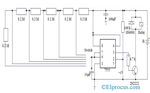
30 Minute Timer Circuit Using 555 Ic And 7555 Ic

Pin On Electronics Knowledge
30 Minute Timer Circuit Using 555 Ic And 7555 Ic

Circuit Diagram Of Ic555 In Astable Mode The Circuit Was Used As A Download Scientific Diagram
555 Timers 556 Timers 7555 Timers Basics Features And Application
1
Ic 555 Timer Pin Daigram With Configuration And It S Applications
1
555
Ic 555 Timer Pin Daigram With Configuration And It S Applications

Pdf Study Of Timer Ic 555
Ic 555 Timer Pin Daigram With Configuration And It S Applications
Ic 555 Timer Pin Daigram With Configuration And It S Applications

Monostable Of 555 Timer Circuits Download Scientific Diagram

The General 555 Timer Circuit Schematic At The Heart Of The Circuit Is Download Scientific Diagram